5 (217) · $ 15.50 · In stock
Description

Two dimensional semiconducting materials for ultimately scaled transistors - ScienceDirect

Surface Analysis of WSe2 Crystals: Spatial and Electronic Variability

Ohmic contacts between monolayer WSe2 and two-dimensional titanium carbides - ScienceDirect
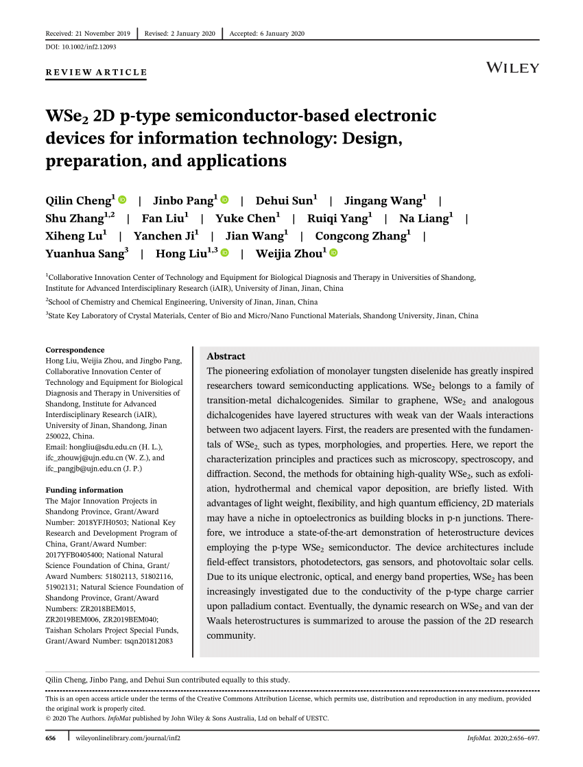
Layer-dependent Schottky contact at van der Waals interfaces: V-doped WSe2 on graphene

Full article: Pseudo-transistors for emerging neuromorphic electronics

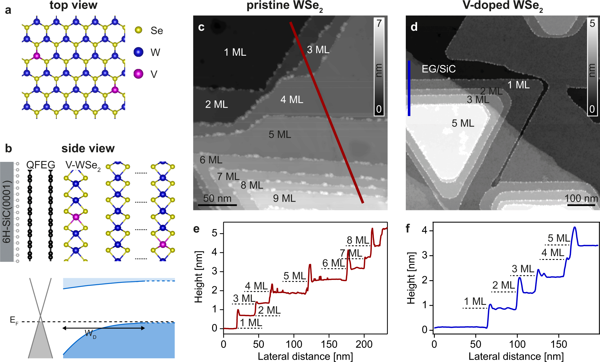
PDF) WSe2 2D p-type semiconductor-based electronic devices for information technology: Design, preparation, and applications

Physical Review Materials - Two-Dimensional Materials and Devices
Controlled edge dependent stacking of WS2-WS2 Homo- and WS2-WSe2 Hetero-structures: A Computational Study
Two-Dimensional Tellurium: Progress, Challenges, and Prospects

Thickness dependent electrical transport properties for few-layer WSe 2

PDF] High performance WSe2 p-MOSFET with intrinsic n-channel based on back- to-back p–n junctions
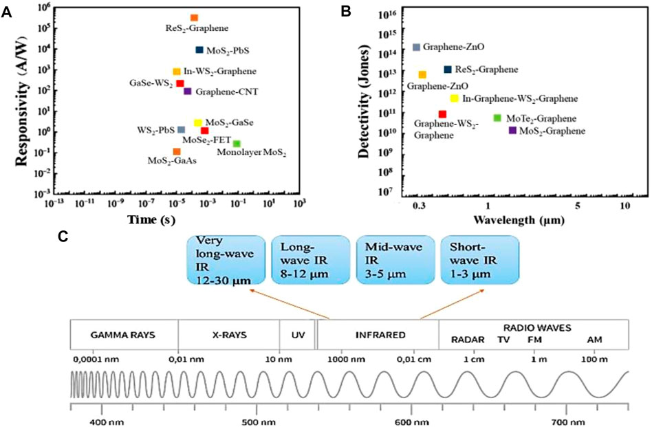
Frontiers 2D Materials for Efficient Photodetection: Overview, Mechanisms, Performance and UV-IR Range Applications

PDF) WSe2 2D p-type semiconductor-based electronic devices for information technology: Design, preparation, and applications